Graphene Analysis with Atomic Force Microscope (AFM)
Three-dimensional (3D)-AFM image of 2D materials-water interfaces. Figure 1 shows some 3D-AFM images of the 2D material-water interface for graphene (Fig. 1a), few-layer MoS 2 (Fig. 1b) and.
(a) A tapping mode AFM image of graphene oxide (GO) sheets on mica
Atomic Force Microscope Images Nanosurf AFMs are used for applications ranging from material characterizations to biological samples like live cells. On this page you can browse the gallery of all our published atomic force microscopy images.. Graphene like C3N imaged in scanning thermal microscopy (sThM) mode dsDNA imaged in dynamic force mode

AFM image and height profiles of exfoliated graphene sheets using LPE
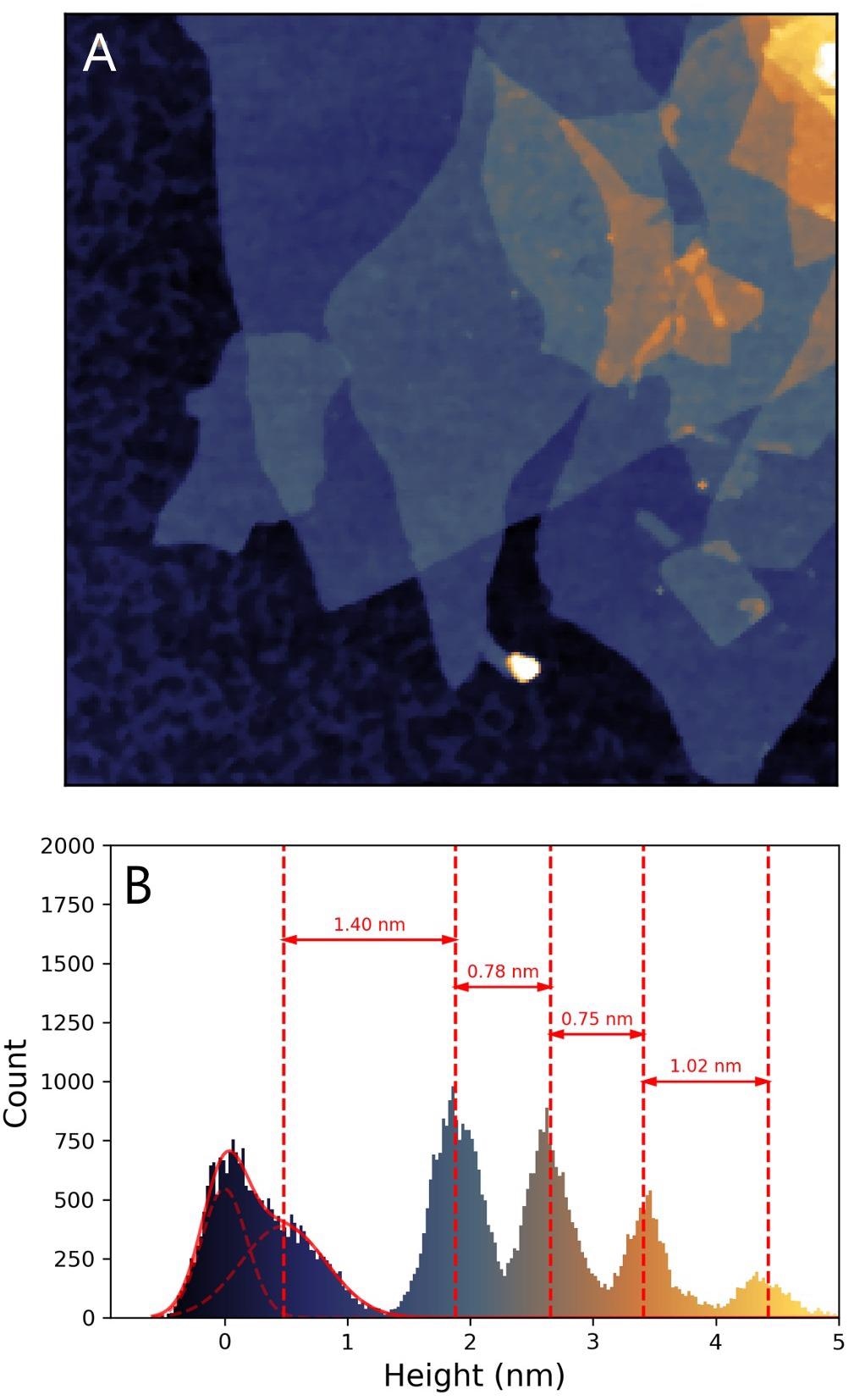
Previous studies using AFM analysis have shown that the thickness of monolayer graphene nanosheets, and the inter-layer spacing are about 0.57 nm, and 0.6-0.7 nm, respectively.

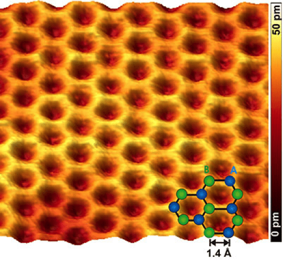
AFM images of representative monolayer graphene (a) and bilayer
AFM topography image of a multilayer graphene flake on Si substrate with lateral dimensions of 10 x 10 µm 2. Cuts were obtained by applying a 10V AC voltage at 500 kHz to the tip of a BudgetSensors ElectriTap190E cantilever (k = 48 N/m nominal) and following the designated path in Static Force Mode with an applied force of 5 µN at a speed of.
Graphene Analysis with Atomic Force Microscope (AFM)
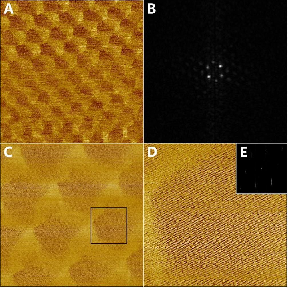
Figure 1: Atomic force microscope (AFM) topography image of a graphene flake (a) and Raman image of the same graphene flake showing the integrated. assign the number of layers that form the studied graphene flake. Numbers in the Raman images in Figure 4 indicate the number of graphene layers. An inconsistency however can be seen in the
The smallest, most affordable atomic force microscope could be a game
FIG. 1: (a) AFM image of an uncut graphene flake (thickness ∼ 5nm). The two-terminal resistance (R) from the left to. FIG. 4: AFM images of line patterns created by the LAO technique. (a) Trenches or bumps were formed on HOPG surface. 6 lines (from left to right) are written with the same tip bias voltage of −20 V while the set point.
Sensors Free FullText MetalloGraphene
Download scientific diagram | AFM images of the structure surfaces: (a) image of the forming fluorinated graphene islands, obtained by printing on a silicon surface; between the islands there are.

(a) AFM topographic image of the graphene on hBN sample in ambient
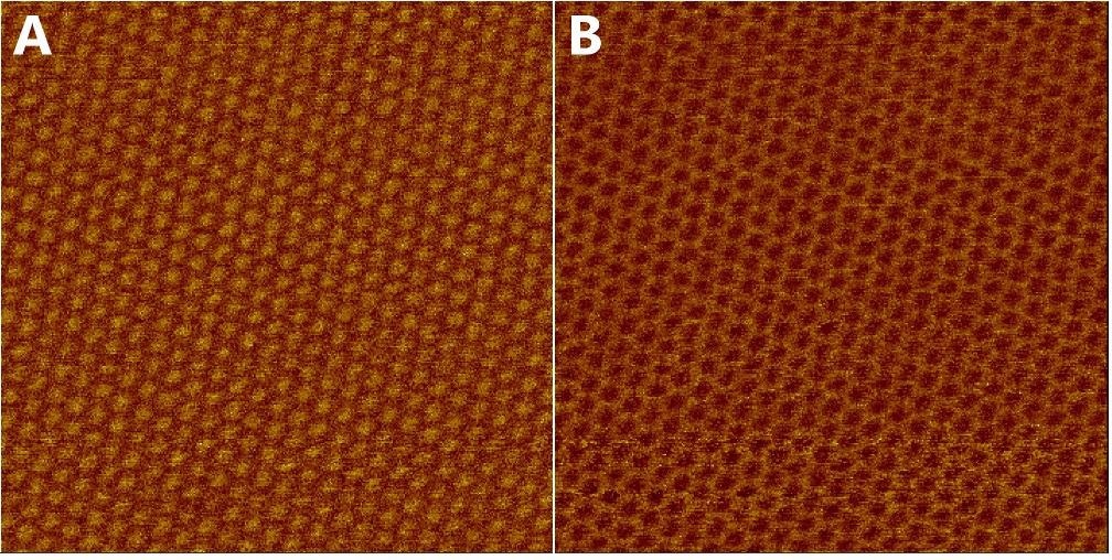
d-f, AFM height images of the corresponding graphene films. The top right corner areas show the correlated AFM phase images from −10.0° to 10.0° of the regions marked in d - f .

AFM images of graphene oxide sheets laying over a Si/SiO 2 substrate
High-resolution AFM images of graphene & 2D materials, sampled using advanced Asylum Research MFP-3D, Cypher, and Jupiter atomic force microscopes.

AFM images of graphene (a) before and (b) after functionalization with
Atomic force microscopy images of graphene oxide precipitate after 4 krpm centrifugation with the presence of aggregates (a), the same after mild sonication (b), precipitate after 8 krpm.
Graphene Analysis with Atomic Force Microscope (AFM)
The atomic force microscopy (AFM) is a direct and visual analytical method to examine the topographical and cross-sectional features of graphene materials. In this study, AFM was carried out, in parallel to HR-TEM, to determine the number of GO layers. Fig. 4 shows the AFM images of GO sheets exfoliated in different polar solvents. In general.

Graphene constriction (a) AFM image of the studied device. (b) Scheme
Figure 2a shows the AFM images of graphene before and after plasma treatment with optimized conditions. After plasma processing, graphene has a smoother surface with less roughness, which.

(a) AFM topography of graphene on hBN. (b) AFM topography of graphene
Download scientific diagram | AFM images of representative monolayer graphene (a) and bilayer graphene (b). (c) AFM image of a largish bilayer with a monolayer lying on it. The histogram gives.

AFM characterization on dispersed graphene sheets. (a) A representative
Figure 3: AFM images and height profiles of graphene on a SiO 2 /Si wafer transferred by our face-to-face technique. a-c, AFM images of films transferred in room-temperature (RT) water (a);.

Typical AFM image of graphene oxide sheets and corresponding height
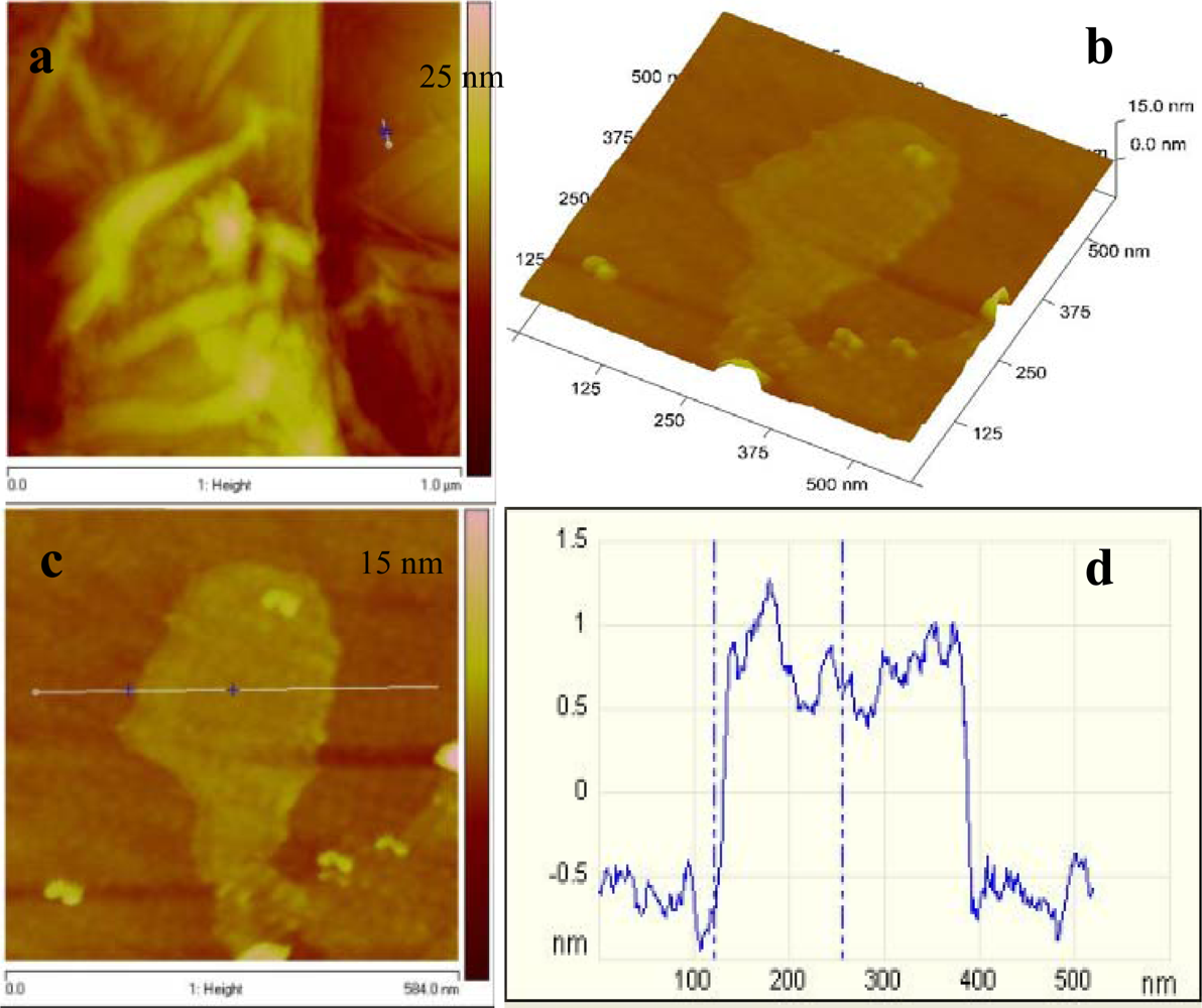
Atomic force microscopy (AFM) is utilized in determining the surface structure and thickness of graphene [84]. An AFM generates images by scanning a small cantilever over the surface of a sample. The sharp nanoscale tip at the end of the cantilever contacts the surface, thus bending the cantilever and changes the amount of laser light reflected.

AFM images of graphene on (a, c) approximately 30 nm Au NPs and on (b
Advanced property measurements have played a key role in the exciting AFM discoveries in graphene research. This research includes quantitative mechanical property mapping with Bruker's exclusive PeakForce QNM ® as utilized by Chu et al (J. Procedia Eng 36, 571 (2012) for unraveling graphene layering and by Lazar et al (J. ACS Nano ASAP 2013) for quantifying the graphene metal interactions.